PCB Scanning - Reverse Engineering
PCB SCANNING TO CAD
Bespoke service
AN ALTERNATIVE TO THE LENGTHY RE_DESIGN PROCESS !
Tired of working with films? Need digital data? Or lose your CAD-generated files? Instead of enduring a lengthy and expensive redesign process, allow our Service Bureau to produce the necessary data. Send us your films, hand-taped designs, diazo film, actual PCB's or technical drawings. Our Service Bureau scans and creates production files from each of these types of media
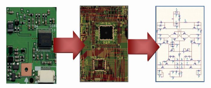
SCANNING - FROM PCB BACK TO CAD
We can scan and engineer your projects directly back into your chosen CAD formats. All we need to supply you with a customised quotation is a copy of your project – quotations are returned by email/fax within a few minutes of their request. If you have a specific request, the service bureau can place your design on grid, make revisions to silk-screens, verify tolerance levels, compare actual PCB's against GERBER images or contrast different design revisions. We have many tools available to us, so please ask if you have specific requirements. Quality Assurance is important to us –it’s the #1 priority of our Service Bureau. That's why each job processed by our service technicians undergoes a detailed quality check ("QC") procedure. Please call today to find out how our Service Bureau can help your drawing office.
SECURITY
An added security feature of the Service Bureau is that complete copies of all jobs processed are stored on-site for five years. If a disk is accidentally erased or misplaced, our service technicians will immediately send you another copy of your completed job together with all documentation !
BENEFITS
- Supply production with required GERBER data.
- All essential files provided by one service centre.
- Improved board quality: Verifiable inter-layer pad, tooling hole and board edge alignment.
- Prevent film/drawing deterioration by storing images on disk.
- Store multiple copies of designs on disk, both on and off-site.
ADDITIONAL SERVICES
The flexibility and power of the system also gives us additional services that we can offer. ScanPlace allows us to create fully documented Pick and Place data for many automated assembly machines. ScanStencil gives us the ability to use the scanner as an AOI machine - allowing us to compare etched/cut stencils against original CAD data.
PRODUCTS OFFERED
- Reverse Engineering
- PCB Scanning
- AOI Inspection
FORMATS INCLUDE
- Film
- Artworks
- Drawings
- PCB’s
- Diazo Film
- Prints
- Screens& Stencils
MAJOR POINTS
- Fast Turnround
- Low Cost Technology
- Quality Assurance

SCAN SPECIFICATIONS
Resolutions: 400, 1000, 2000 dpi
Most scans from films and artworks are done at 1000 dpi. In cases where we need a colourscan for reference from a finished PCB, then we may scan at 400dpi due to file size limitations (Colour scans may create files up to 500 mb in size). 2000 dpi is only used in rare occasions where very thin lines are needed.
Mediums: Pos Films, Neg Films, Diazos, Pen plots, Artworks, PCB’s, Paper Prints
The above are in order of preference. Formats other than Pos Films will incur some set-up charges.
Accuracy
The actual positional accuracy of the scanner is +- 0.002” overall. We use a glass master grid to calibrate the scanner every 12 hours. However, you may sometimes find items placed or sized outside of these tolerances. This is because of the way that the software interprets the raster, and the way that it re-routes tracks and re-aligns pads together from layer to layer. For example, if we scan a hand taped double sided artwork, the second layer is not mapped to the master, but instead mapped to the first layer. This effectively means that we are tidying up and registering layers together. All layers undergo a rigorous inspection method (see below).
Return of Data
Once data is ready to return, we prefer to send the data back by email. Master films/artworks are then posted back for a guaranteed morning delivery, at a cost of £6.65 nationally, unless otherwise requested.
Data geometry / format
All data sent back, unless otherwise requested, will be Gerber 274-X files, along with Excellon 2.3 imperial drill files where requested. The notes below are just a guideline. Different technology on a board, and different actual master formats, means that the type of data returned to you may vary quite widely in the geometry used. All data formats will, however, be fully compliant with modern CAM and Photoplotters.
TRACKING: If the PCB type was originally CAD drawn (45/90 deg tracks) then the track layers will mostly be made up of single draws for the tracks, and single flashes for the pads. This is very clean CAD data, quite often as if it had come straight from the PCB designer. If the PCB type was originally hand drawn (curly tracks) then they will usually be created as polygon or bitmap draws with flashed pads buried within the copper where possible. If you need your data formatting
differently to this, then please let us know before we process the job. IDENTS: These are usually created as ‘bitmap’ Gerber’s, and effectively will be built up out of lots of small lines MASKS: Will be single flashes where possible
INNER PLANES: If these contain just pads with thermals, then they will be made up of negative flashes. If they are mixed planes with signals on, then they will either be generated the same way as normal outer tracks, or created as composite layers.
Inspection Procedure
- Once a Gerber file has been created from the raster data, we first of all run OVERPLACEMENT CHECK (usually at MEDIUM resolution of 0.004") This will look for any raster data that hasn't got Gerber data on top of it, and also any Gerber data that hasn't got raster data underneath it. Errors are highlighted on screen. This basically makes sure that we haven’t missed/added anything.
- Then we run a VERTEX JOIN - this extends any track that touches a pad and makes it snap to the centre of the pad.
- Then we run VECTOR CHECK - this looks for any track that doesn't join other tracks or pads neatly and highlights them on screen.
- Then we run OVERPLACEMENT CHECK- FINE. This is the same as our first check, but we set a tolerance to look for smaller items (up to 0.002" where design constraints allow).
- Then we run SPACING CHECK which runs a basic space check. We select a gap to look for depending on the type of board and the smallest track size. (We normally check these at 0.010")
- Finally, after the whole job is finished, we do a TEST PLOT on our photoplotter and physically overlay a film plot against the master, and these are inspected by eye.
The above inspection procedure is for a standard scan application. However, there are constraints on some jobs where
not all of these procedures can be ran. For example, if we are to scan a physical PCB without stripping it, then not all of
the above procedures can be carried out because of the lack of raster data to compare to.
Dimensioned Drawings
If dimensioned drawings are supplied to us, we will not check tolerances or dimensions of the scan to the drawing unless
specifically requested to do so. When scanning a master, we are effectively being contracted to copy the master
supplied. If this master doesn’t dimension correctly to a drawing, then editing the scan to fit would be classed as a
modification, for which we charge extra by an hourly charge.
Scanning from PCB’s
The procedure to scan from a finished PCB is quite time consuming. Firstly we take a colour scan to use as a reference
layer. Then the board is chemically etched to remove the solder mask and silk screen layers. Depending upon the finish
and style of the board, we sometimes then Tin/Lead strip to get back to bare copper, and in rare cases we also apply a
black oxide finish to the copper to give us good contrast. If we are to produce drilling from the board, remember that we
are copying the master board given to us, which perhaps will differ from the designers intended layout, so drill
wander/deflection and plating thickness’ all can alter the positional accuracy of the drilling. The same goes for
routing/profiling. We are , in effect, copying a produced circuit rather than re-creating the designers original design.
Turnround
We aim to turn each job round, from receipt of artworks, within 3 days. We are able to return data more urgently than
this if requested. For scanning from films, we are effectively able to offer a sameday service if the job is very urgent.
However, even though we have 2 systems operational for scanning, there are times in the month when some jobs on
standard turnaround may take longer than 3 days.
Important
Although every possible care and attention is given to our work, please ensure that you check this data out thoroughly
before use. If our work is found to be faulty, we will rework/replace/credit this job. We shall not be liable for any direct,
consequential or incidental loss or damage resulting from the use of this data. We expect you to make prototypes /
samples only from this data to ensure the data is correct prior to manufacturing. The process of recreating CAD
layouts from minimal information is a complex one and errors can be made
FAQ's
Q: What is the accuracy of the scan ?
A: This depends upon the resolution that we image at, the material that we image at, the tone of the mask, and most importantly the feature type (Spot, square, line etc). This all makes it very hard to give a figure, but as a very rough guide we can make 2-3um on an "everyday" basis and down to 1um and possibly below if we "hold it's hand through production".
Q: How big a scan can you perform ?
A: This is dependant upon the resolution that we image the mask at. The QUICK REFERENCE brochure in the DOWNLOADS section will give you a chart, specifying both feature and dimensional tolerances.
Q: Can you scan physical PCB's?
A: The higher the resolution, then the sharper the edges of the features, the smaller the features possible, the more accurate the features will be, the sharper the corners in of the features, and also the smoother the circles. Some customers will notice this difference straight away, some will hardly notice any difference. Every customer has different requirements and different priorities. If in doubt, chose a higher resolution to ensure your requirements are met, but we are happy to advise if you send us your database.