Metal Backed PCB Quote
PCB Quote Request
Metal Backed Technology
METAL BACKED PCB’S
The rise in LED technology from conventional bulbs and lamps has necessitated the need for PCB’s to be able to counter the heat generated by LED’s.
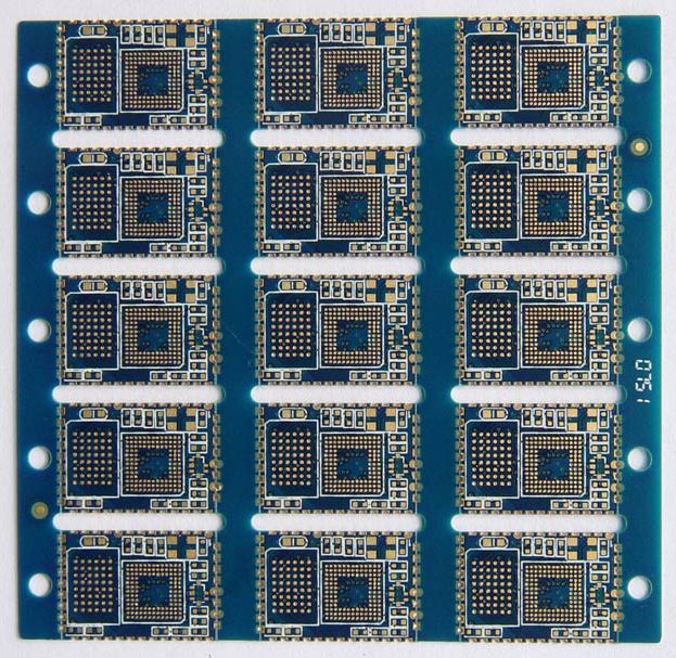
Standard FR4 boards on their own tend to burn and subsequently fail in high temperatures. Therefore, to alleviate this issue metal backed PCB’s are used which in essence are thin PCB’s bonded with either Aluminium or Copper of varying thicknesses. The result of this backing means that any excess heat passes through the FR4 substrate and is sucked in by the Aluminium or Copper thus stopping the actual PCB from over-heating.
Just tell us your exact requirements above or give us a call on 01462 452616 to speak with one of our PCB specialists.
Metal Backed PCB’s
Technologies
- Conventional
- Plated Through Hole (PTH) & Multilayer
- Ionic Test Report
- High Aspect Ratio Plating
- High Copper Weight for inner & outer layers
- Thermal Management
Materials
- IMS (Aluminium, Copper Board)
Finishes
- HASL
- ENIG
- OSP
- SILVER
- Tin
- Palladium
- Carbon
If you require clarification, please either email or click for LIVE SUPPORT.
How quickly can I have my PCB's (Printed Circuit Boards)?
Our standard delivery for landed offshore boards is 15 days but you can choose from 24hrs, 3-day, 5 day and 10 day landed deliveries. We also offer both scheduled and consignment stock services so for large quantity orders not required on a one drop delivery, we will store your boards for up to 12 months free of charge.
What size PCB's (Printed Circuit Boards) can you produce?
PCB's are used in a large variety of electronic products and therefore need to be produced in lots of different sizes. As a guide we can go as small as 5mm square, up to back plane products, just tell us the exact size you require, and we will produce it for you. There are several factors to consider including the size of the product, single sided, double sided, multi-layer as well as the number and size of the components to be soldered on. For information and assistance please call us on 01462 452616 and speak to one of our experts.
Can I have my PCB's (Printed Circuit Boards) in different thicknesses?
PCB's come in a variety of thicknesses to accommodate a multitude of products and requirements. 1.6mm is the standard thickness for multilayer boards but we can produce from 0.4mm up to 3.2mm. Just tell us your requirements when requesting your quote and we will be happy to advise accordingly.
Can I have my PCB's (Printed Circuit Boards) in different colours?
Our standard colour solder resist is green but there are other colours available, red, black, blue and white. We appreciate the colour of the photo resist is very important especially if the board is going to be on display as in lighting, hi-fi equipment or consumer electronics. Just let us know what colour you require and we will be happy to produce this for you.
What finishes can you produce on your PCB's (Printed Circuit Boards)?
Our standard finish is HASL (Hot Air Solder Levelling). This is where the PCB's are immersed in molten tin alloy and the HASL machine then removes any excess with a blast of hot air. This leaves the surface mounts smooth and flat for soldering. HASL is lead free and compliant with RoHS (Removal of Hazardous Substances) regulations.
We can also finish boards in Silver, Nickle, Palladium, ENIG (Electroless Nickel Immersion Gold) and OSP (Organic Solderability Preservative)
What is the smallest hole size I can have on my PCB (Printed Circuit Board)?
The finished diameter of a hole is determined after the plating and surface finish has been applied. The smallest hole size is 0.2mm and the designer of your PCB will determine this. The actual drill size is always larger than the finished diameter because drilling takes place before plating and surface finishing, so we add 0.1mm to the required finish size to allow for this fact. If you are in any doubt about the hole sizes please call us on 01462 452616 and speak to one of our PCB experts.
What information do JD Photodata require from us?
We require Geber files in order to process your order. This can be either supplied by yourselves or we can produce them for you based on your circuit diagram and component list by providing a CAD image in-house. We can also design PCB's if you have an existing circuit that needs reproducing or from historic designs. We also offer Reverse Engineering services which enables us to scan old boards with no available data in order to produce the exact same board. Our skilled engineers will be happy to help you every step of the way.
Do I need to open an account to place an order with JD Photodata?
No. We will automatically open a customer file in your name to keep track of quotes, orders and deliveries but this is not a payment account. On your first order we will issue you with a pro forma invoice that would need to be paid when your order is placed. Any future payments will be invoiced once we have delivered your goods. We accept Visa, Mastercard and Paypal.


