How are Photomasks Used?
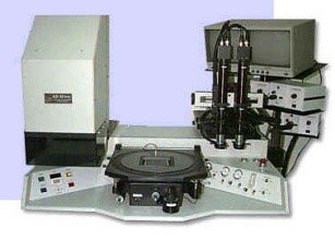
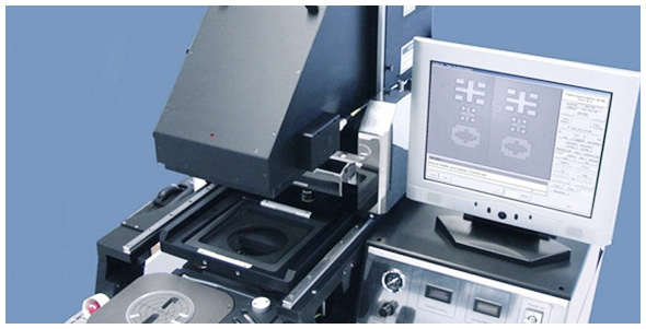
Our glass masks are used in a variety of different applications and processes, but one of the most common procedures is to use the mask in a ‘mask aligner’. One of the most important steps in the photolithography process is mask alignment.
The mask is aligned with the wafer so that the pattern can be transferred onto the wafer surface. Many MEMS devices are made with multiple materials and multiple layers, so in that case, each mask after the first one must be aligned to the previous pattern for the device to work correctly. Sometimes the alignment between these layers is supercritical, and complex expensive machinery is required.
Once the mask has been accurately aligned with the pattern on the wafer's surface, the photoresist is exposed to the pattern on the mask with a high-intensity ultraviolet light. There are three primary exposure methods: contact, proximity, and projection.
CONTACT PRINTING
In contact printing, the resist-coated silicon wafer (or other substrates) is brought into physical contact with the glass photomask. The wafer is held on a vacuum chuck, and the whole assembly rises until the wafer and masks contact each other. The photoresist is exposed to UV light while the wafer is in contact position with the mask. Because of the contact between the resist and mask, very high resolution is possible in contact printing (e.g. 1-micron features in 0.5 microns of positive resist). The problem with contact printing is that debris, trapped between the resist and the mask, can damage the mask and cause defects in the pattern.
PROXIMITY PRINTING
The proximity exposure method is like contact printing except that a small gap, 10 to 25 microns wide, is maintained between the wafer and the mask during exposure. This gap minimizes (but may not eliminate) wafer damage. Approximately 2- to 4-micron resolution is possible with proximity printing.
PROJECTION PRINTING
Projection printing, avoids mask damage entirely. An image of the patterns on the mask is projected onto the resist-coated wafer, which is many centimetres away. In order to achieve high resolution, only a small portion of the mask is imaged. This small image field is scanned or stepped over the surface of the wafer. Projection printers that step the mask image over the wafer surface are called step-and-repeat systems. Step-and-repeat projection printers are capable of approximately 1-micron resolution.