
Where are Photomasks Used?
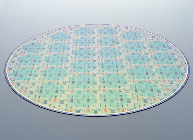
Photomasks play the role of photographic negative film in the manufacturing of devices such as chips or LCD panels. Chrome plates are commonly used as the choice of substrates on which detailed images or patterns are formed, although polyester films are also common in low cost / low technology applications. The patterns or images are then transferred onto the wafer surfaces by shining lights through the photo-mask plates, just like the negative films that are used to project images on to photographic papers. Since the precision and accuracy of the pattern geometry on the photomask affects device quality, the photomask is considered as a key integral part of overall semiconductor technologies.
Photomasks are used in wafer fabrication, microfluidics, strain gauges, MEMS, Optics, flat panel displays, BioMed, PC boards.... but are also used in many other applications by a wide range of industries and technologies.

